Huawei has been one of the top players in the mobile chip designing for years, and its research on new designs has continued to evolve amid the US ban. Recently, a chip patent has surfaced on the internet, making a buzz around Huawei’s potential adoption of 2nm processing technology in the near future.
HiSilicon, Huawei’s chip designing department, has been handling all the heavy work; it designed Kirin chips for smartphones. In 2019, it lost access to printing new processors through Taiwan’s TSMC, crippling HiSilicon‘s market presence.
However, the recent arrival of Huawei’s homegrown chip manufacturing has raised eyebrows. Somehow, it has returned the Kirin from the dead and launched new smartphones with 5G capabilities.
But the doubts remain on the processing node, as some previous report claims the company is still using 7nm tech to make a new chip. That’s years behind the likes of 2nm and 3nm chipsets made by Samsung and TSMC. That goes for both performance and efficiency.
However, Huawei, with its homegrown HarmonyOS operating system, has managed to provide both negligible performance and high power efficiency through deep hardware and software collaboration.
While Huawei is making progress in its chip development camp, a patent for a potential 2nm node has appeared online. Here is some important stuff that we’ve gathered about this technological breakthrough.
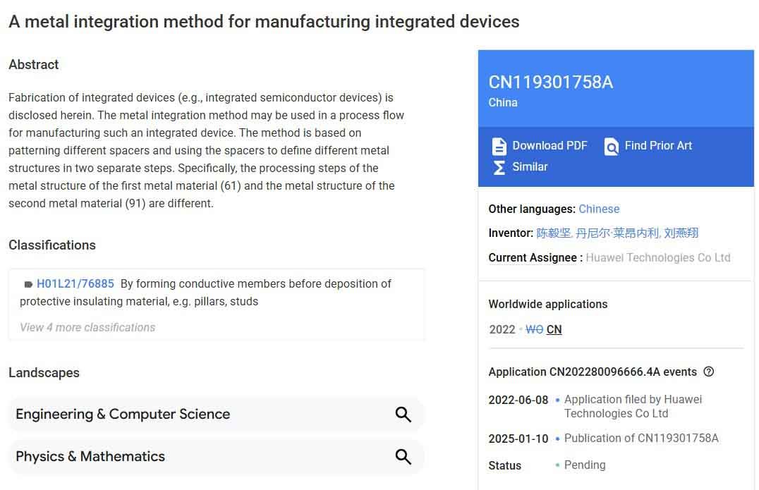
The patent (CN119301758A) is titled “A metal integration method for manufacturing integrated devices”. It was filed on June 8, 2022, under the application CN202280096666.4A with the China National Intellectual Property Administration (CNIPA). It was officially published on January 10, 2025, with classifiers such as interconnections and dielectrics, which generally align with semiconductor manufacturing processes.
Supporting advanced nodes: The patent targets metal pitches below 21nm. Its process aligns with the interconnect densities required for both 3nm and 2nm-class nodes, but doesn’t specifically mention any advanced process technologies.
Spacer-based patterning – The patent introduces a multi-layer spacer scheme using five distinct spacers to define narrow metal structures in two sequential steps. It enables precise gap formation for metal deposition without relying on EUV lithography, which is ideal for sub-21nm pitches in foundry BEOL processes.
Dual-Material Metal Sequencing – It separates the integration of the first metal, such as ruthenium or copper, and the second metal (cobalt) into processing phases. It completes the process by first filling gaps after removing inner spacers and cores, and then etching trenches in a dielectric-filled second gap. Overall, it improves robustness against edge placement errors (EPE) below 5nm.
FSAV – A selective etching process forms self-aligned vias by creating openings in spacers via photolithography, extending into the substrate for first and second vias, leveraging the high etch selectivity of hard masks to minimize misalignment in advanced interconnects.
Area-Selective Deposition (ASD) for Hard Masks: Recessed metals are capped with dual-material hard masks deposited selectively via ASD through protective layers to prevent over-etching. This is crucial for maintaining integrity during FSAV fabrication in high-density foundry lines.
DUV-Compatible Narrow Pitches: The method achieves metal pitches under 21nm (or even <32nm) using deep ultraviolet (DUV) patterning alone. It bypasses EUV costs and improves EPE margins via spacer protection, making it a highly scalable solution for next-gen foundry products.
Applications: It applies to substrates with middle-of-line (MOL) or back-end-of-line (BEOL) layers, including IC power rails. The process includes filters and third dielectrics to block unwanted deposition, yielding integrated devices with reduced capacitance and enhanced performance.

Conclusion
This patent has much potential and improves the chip manufacturing process by enabling ultra-fine metal lines under 21nm using affordable DUV lithography, skipping EUV costs.
However, the question remains whether Huawei’s HiSilicon department will utilize this patent to generate a 2nm chip? We’ll have to find out the answer to this question.
The post Huawei’s 2nm Chip Patent: 7 things you should know appeared first on Huawei Central.