Andrew B. Kahng, a well-known US chip scientist, has said that Huawei’s path to the 1.4nm chip development is possible through non-traditional ways introduced by Tau (τ) Law.
Andrew B. Kahng is a Distinguished Professor of Computer Science and Engineering (CSE) and Electrical and Computer Engineering (ECE) at the University of California, San Diego (UC San Diego).
He holds the endowed chair in high-performance computing and is a world-renowned expert in Very Large Scale Integration (VLSI) electronic design automation (EDA), integrated circuit (IC) physical design, and semiconductor technology roadmapping.
The scientist said that Huawei’s technology roadmap can achieve a short research and development cycle compared to existing technologies in some core dimensions as a reaction to Huawei’s new Tao Law.
Last month, He Tingbo, Huawei’s chip design lead, announced Tau (τ) Law. This is the company’s technological roadmap to overcome semiconductor manufacturing challenges by shrinking the physical size of transistors.

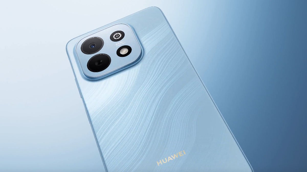
(Image Credits: Huawei)
The first chip with this new architecture will be released later this year. By 2031, Huawei plans to launch a new chip with a transistor density comparable to that of a 1.4nm process with traditional technologies.
In a comment posted by mydrivers, Kanhng pointed out that Huawei has five years to leap through 1.4nm tech. It should be safe to assume that Huawei may have fully mastered a verifiable path to support the process application. This suggests that the relevant core research has advanced to a fairly mature stage.
The semiconductor industry has been witnessing that the marginal benefits of advanced process upgrades continue to narrow. Meanwhile, the improvements in each generation of upgrades derive from three areas: power efficiency, performance, and the leap from technology process, such as from 5nm to 3nm, 2nm, and then 1.4nm.
Therefore, the technological gap between Tau’s Law and traditional processes will continue to narrow in the near future. Hence, the success rate of a non-traditional path is much higher than what observers previously predicted.
The post Top US chip scientist said Huawei’s 1.4nm chip path is possible: Report appeared first on Huawei Central.