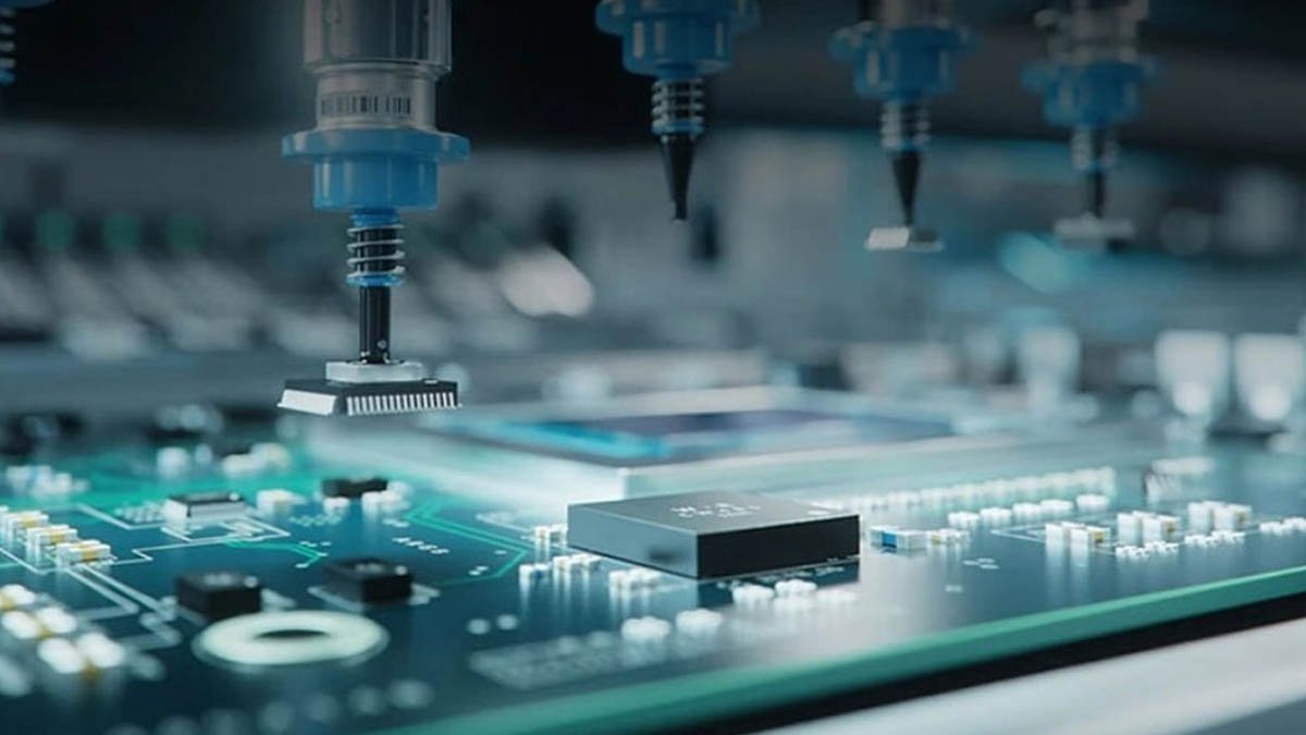
Huawei’s latest chip innovation is in the limelight at the moment and Peking University has now revealed those 3D design tools that are fueling this advancement. Here’s one of the significant secrets behind the tech giant’s new mobile chip technology.
Peking University is one of the most elite research universities in Beijing, China. It is considered the top academic institution in the country and ranks among the leading universities around the world.
Researchers of Peking University have now announced that their newly-made 3D design tools power up Huawei’s chip innovation – the new LogicFolding architecture.
According to the details, top researchers at Peking have developed a brand-new prototype of EDA to frame out LogicFolding and bring Tau Scaling Law into action.
These 3D tools are generally a prototype for Electronic Design Automation (EDA) – a highly specialized software used to lay out and evaluate microchips before they are fully developed and ready for integration inside the device.
While Chinese Huawei can’t access cutting-edge technologies, it has focused on developing its own solutions. Peking University’s EDA tool complies with Huawei LogicFolding Architecture.
How does it work?
Researchers call the new EDA prototype a true 3D method. It addresses the multilayer chip as a single structure during the design process. As a result, it allows for optimizing the entire vertically-arranged group to deliver even better performance.
According to the university, when researchers tested their prototype on an open-source industry-grade chip design, it achieved 30% reduced wire length inside the chipsets, while improving performance and heat management over outdated methods.
Simply put, instead of mapping out each 2D layer like designing a skyscraper floor by floor, before stacking them on top of each other, the latest EDA treats a multilayer SoC as a single layout.
Huawei revealed that its chip ambitions still contain many challenges. But things will be slightly less problematic compared to the past few years. He Tingbo, the President of Huawei’s Semiconductor Business, said:
“If we look at the upcoming decade, no single company can address all these challenges alone.”

(Image Credits: Huawei)
The post Huawei’s chip innovation is fueled by these 3D design tools: Report appeared first on Huawei Central.