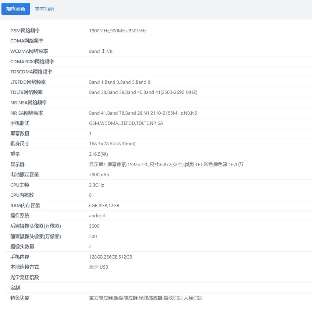
Huawei has just teased a major chipmaking breakthrough coming this fall – LogicFolding Architecture. The company says that the 2026 Kirin processors will help it overcome the US clampdown and, once again, gain the real power of 5G mobile chips.
But the question is – what is Huawei LogicFolding Architecture? Let’s check in detail.
LogicFolding is Huawei’s new technical approach to open innovation for its smartphone chips. Instead of following Moore’s Law, which has been ruling the chip industry for almost five decades, the company has adopted a new τ Scaling Law.
Over time, Moore’s Law led to severe physical limits that reduced economic growth. Besides, the geometric scaling of transistors slowed down and urged the need for a new tackle system for the common challenges.
Well, Huawei now has a way to address these issues. The Chinese tech giant has come up with a new chip tech solution called LogicFolding, based on the τ Scaling Law.
Note that the company has already mass-produced 381 chips based on the τ Scaling Law. But it will be the first time this year that Kirin 5G processors will use LogicFolding.

Huawei Kirin 5G chip
It is a multi-level co-optimization premium setup that focuses on systems, chips, semiconductor devices, and circuits. It mainly targets the reduction in the time constant τ to accelerate the performance, energy efficiency, and transistor density.
The LogicFolding chip design works in four ways: device level, circuit level, chip level, and system level, enhancing the performance in every aspect. These are:
- Chip Level: Employs full-stack coordinated design of software, architecture, and silicon to achieve fine-grained, workload-driven control over instruction and data flows, enhancing system-level parallelism and efficiency, and significantly reducing end-to-end execution time.
- Circuit Level: Breaks down the physical boundaries of outdated circuit layouts and minimizes critical-path wiring, reducing the resistive and capacitive load of signal propagation and boosting transistor density + circuit performance.
- Device Level: Optimized the resistance and stray capacitance of transistors + interconnects to minimize the device-level time constant τ at the underlying physical layer.
- System Level: Redefines interconnect protocols for computing systems with UnifiedBus to achieve unified memory addressing and native memory semantics for SuperPoDs, significantly reducing system communication latency.
“We believe that openness and collaboration are key to driving ongoing progress in the semiconductor industry. No single company can independently find all the answers along the path of semiconductor evolution. With the τ Scaling Law, we look forward to working closely with scientists, engineers, and industry partners around to drive the sustainable development of the semiconductor and electronics industries.”
The post Huawei LogicFolding Architecture: Everything you need to know appeared first on Huawei Central.